Reverse Engineering a Graphics LC Display
Introduction
In this article we will explore how I figured out the inner workings of a graphics LCD from old MITEL 52/53xx series desktop VoIP phones. This is not magic folks, this is honest-to-goodness pwning pleasure, reverse engineering of the old-skool kind.
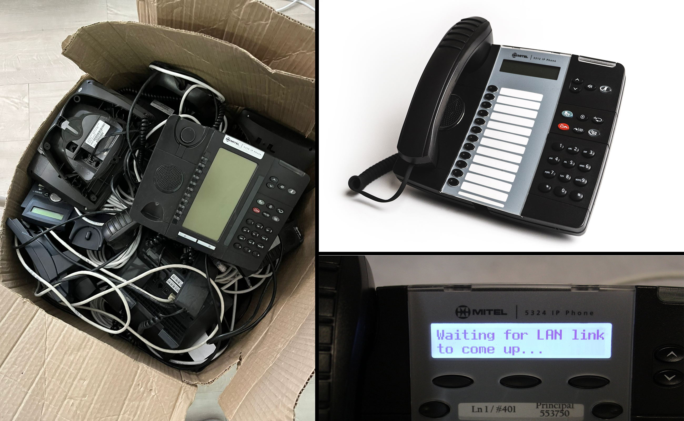
With the demise of MITEL's presence in my country, and the products being replaced by cheaper Chinese product (Yealink), an awful lot of these end up in e-waste. They're everywhere, and the other problem is, they're designed to work with the proprietary MITEL VoIP system. Although they can be configured to work in SIP mode, I was not able to find the firmware for this, and really didn't want to put in all that effort either.
E-Wasted, a box full of 'em
In February 2025, I was buying a USB-C charging cable at the local computer store and saw a huge box full of these phones in their reception. So I asked:
"What's the deal with this box of IP phones?"
"Sir, they're going to be sent to the e-waste"
"Can I have them, please?"
"Yes of course!"
Getting Started
This product contains a LCD display module, a COG (Chip-on-glass) type made by Solomon Goldentek. An e-mail exchange with Solomon Goldentek confirmed the LCD was theirs, however when I asked them if I could have a datasheet or at least know which controller chip was in the display, they told me to get stuffed :/ That's the polite version.
If it was just one phone I would have just thrown it away, but, with so many of these LCDs that could be used again, I decided it was time to get up to some good old hardware hacking!
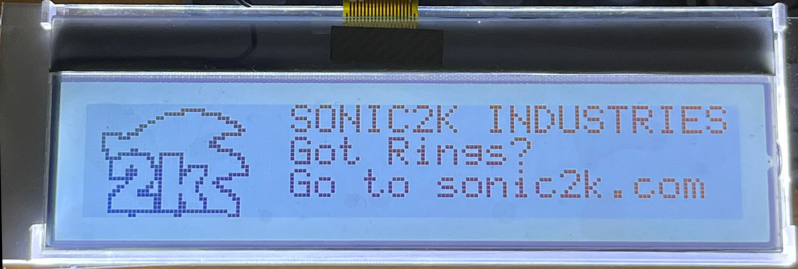
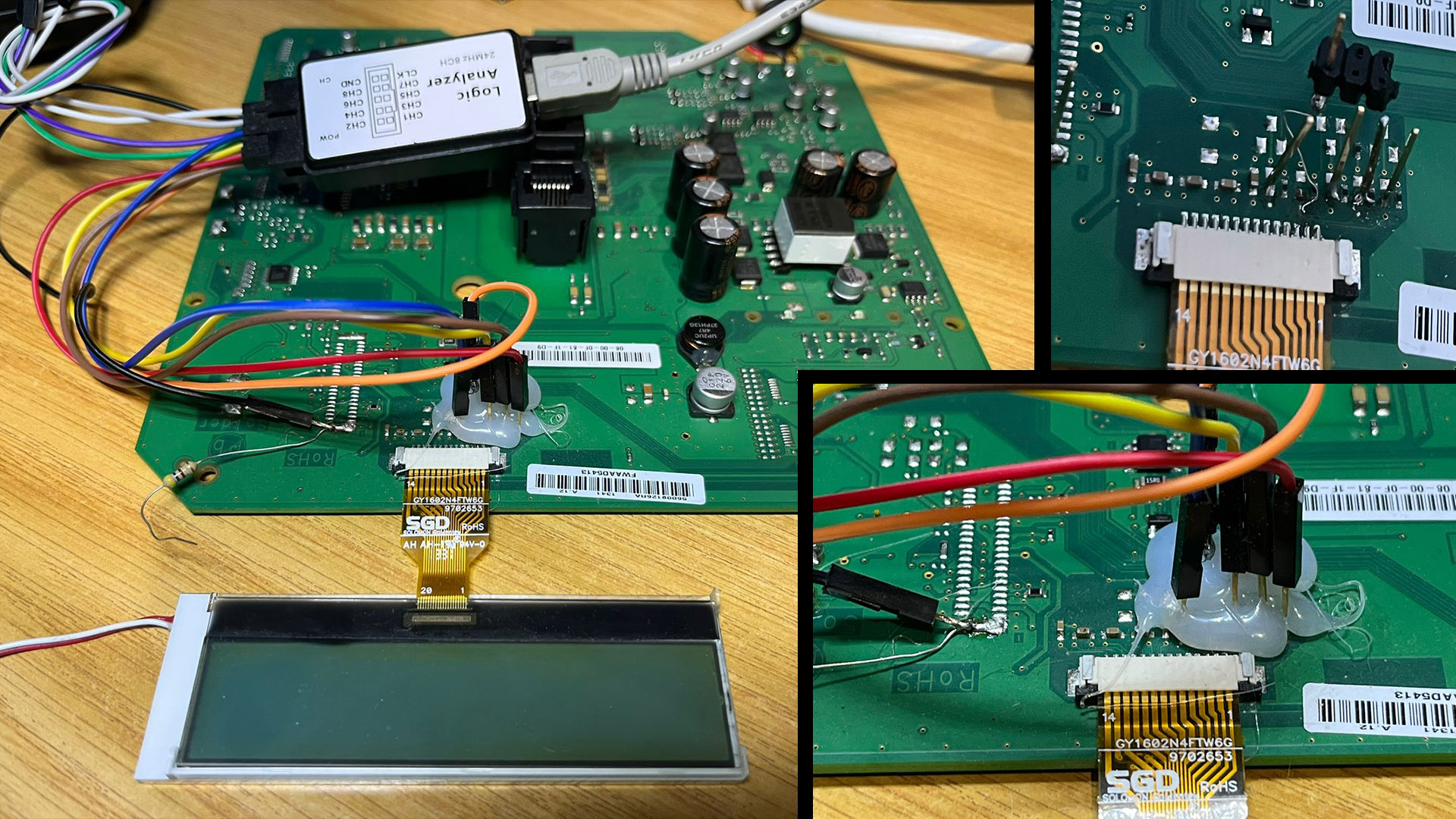
Whenever working with something like this it's always a good idea to get the item that you're hacking, working in it's minimal form. Since I didnt't care for the controls, the handset, or even the speaker and other crap at this point, I tore the phone apart completely and got it down to just the circuit board and the LCD display, working from PoE provided from the Ethernet switch in my home office. Here is what it looked like on my desk, with the bare minimum, but working. The display was alive, and that's what I needed. A working display section so that I could work out the electrical connections.
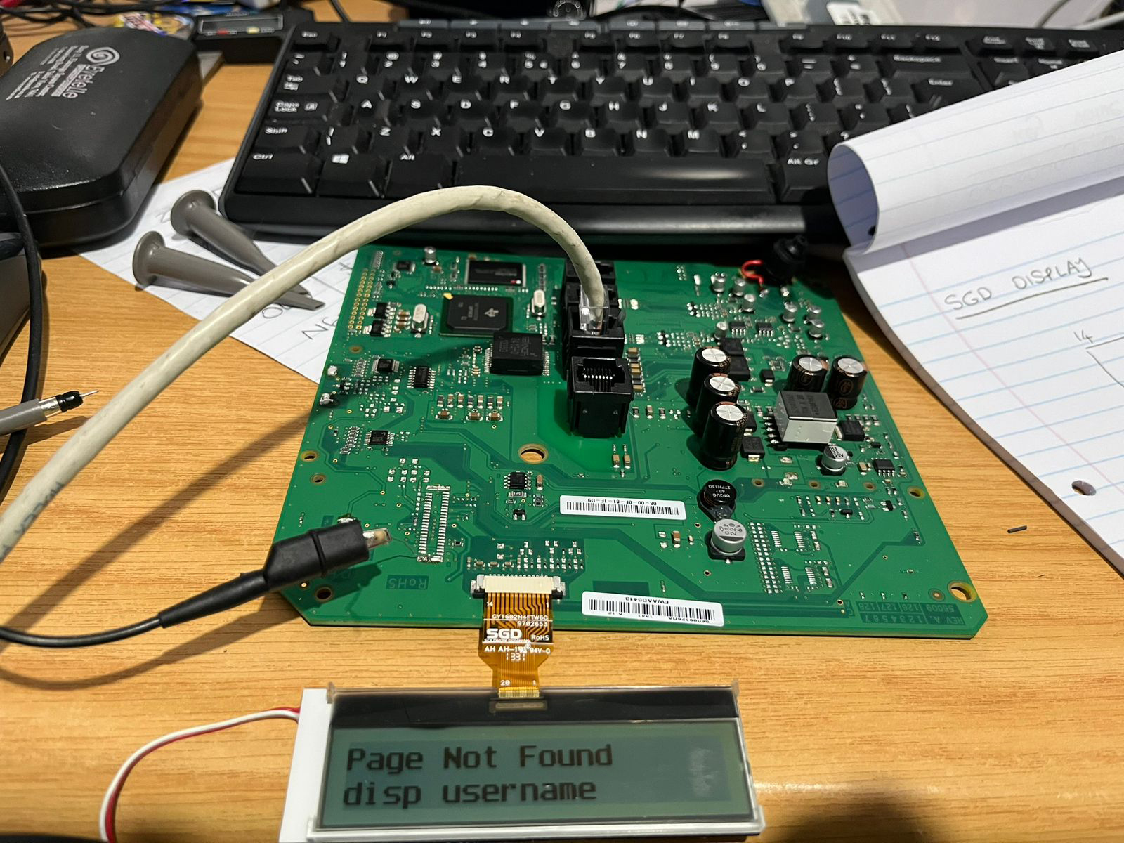
So given the low number of connections on the display it is obvious we're dealing with a serial interface, typically for these kinds of displays being CLOCK, DATA COMMAND/DATA, CHIP SELECT, and the rest being power and voltage divider capacitors.
Using an oscilloscope to probe the pins, and then by tracing the circuit only a little, we find that:
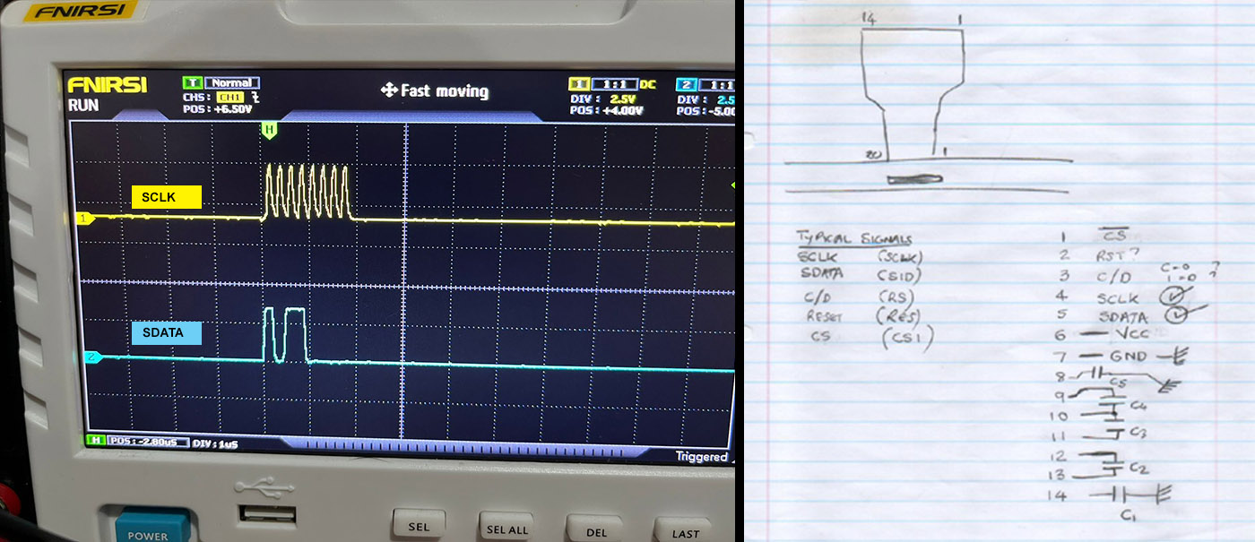
SCLK is 8 pulses, which means 8 bits in a byte, and SDATA changes on the edges of it, which makes it very clear which signals do what. By this method we've clearly identified the two important signals, the others are guesses but we will soon figure them out. Notice the ? marks in my handwritten notes. Vcc is obviously power, a quick measurement reveals 3.3V DC which is pretty typical (because this display hangs off the phone's CPU which itself requires 3.3V DC).
Busting out the Logic Analyzer
Since there are now relatively few unknown signals, we can comfortably use a low cost logic analyzer to see what signals travel to this LCD from power on to fully displayed graphics/text. I used one of the low cost commodity ones that you can buy on eBay and just about anywhere nowadays. To conveniently probe the signals of interest, I added pins onto the phone's board to allow me to jumper into the logic analyzer:
Enter Sigrok PulseView
With the logic analyzer connected, we're in a good position to now capture everything that happens from the moment that power is applied to the board until something is presented on the display, and that's important- once we have captured that initialization and can decode it, we can start looking around at the commands to match up with valid commands of known LCD controller LSIs...
Within minutes, in PulseView, with a sample rate of at least > 2MHz selected, we can see clearly what happens here at power on and set up a decoder to decode the data. It's regular SPI type data so PulseView has a decoder, simply defining SDATA and SCLK in the decoder view, and it decodes the bytes...
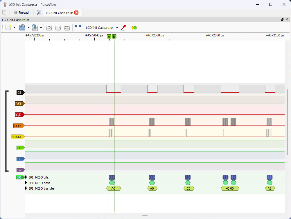
In the above we can see:
* One signal remains high (can only be a RESET signal because making it go low (logic 0) resets the display)
* One signal goes low every time the SCLK signal becomes active: obviously that's the CHIP SELECT
* A bunch of bytes are sent and C/D remains low (because if it's 1- it means writes to DDRAM take place)